 , which
is more than the typical thickness of a thinned CCD.
At short wavelengths absorption occurs near the surface, e.g. at
400nm half of the light is absorbed after 0.15
 .
.
The transparency of Silicon depends strongly on wavelength.
At long wavelengths, QE is low due to a high transparency, e.g. at
950nm half of the light is absorbed at a depth of 36 , which
is more than the typical thickness of a thinned CCD.
At short wavelengths absorption occurs near the surface, e.g. at
400nm half of the light is absorbed after 0.15
 .
.
The potential well of the pixel-defining electrodes does not extend all the way to the surface of the CCD. Photo-electrons generated near the surface may then diffuse to neighbor pixels, causing a degradation of the image sharpness.
In MPP+ mode, the three parallel phases are all ``low'', while in conventional MPP-- mode, one of the phases is ``high''. The high phase increases the attracive force on the photo-electrons, making the diffusion slightly less significant.
The effect of diffusion can be seen in the Point Spread Function
intrinsic to the Silicon, or in it's Fourier transform, the
Modulation Transfer Function.
A thorough examination of the MTF of a CCD is presented at
http://www.astro.ku.dk/ ijaf/mtf/mtf.html, while the method
is described in [Andersen, M. I. 96]. Below, a few results are given.
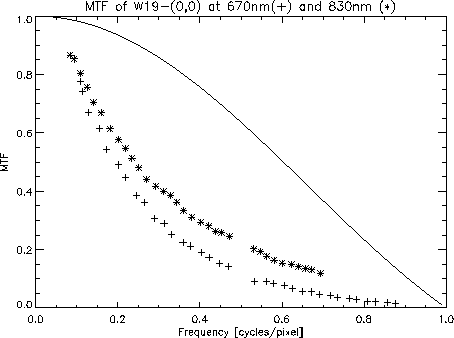
The measured MTF is shown in figure 4 for illumination wavelengths of 670nm and 830nm. In the same figure, the expected MTF due to the pixel geometry is shown. A rather poor MTF is clearly demonstrated. Some instrumental effects are not are not removed from the data, but the impact on the result is minor.
The analysis of the MTF data for the W19-(0,0) has not been completed, but the raw data appears very similar to data for another well examined CCD from the same batch, and data for this CCD is therefore presented below.
The MTF is measured in one dimension, for which the spatial equivalent is the Line Spread Function (LSF). From the LSF, a two-dimensional pixel PSF is calculated. The effective pixel size can be defined in several ways. Here we use the Strehl equivalent width, i.e. 1 / SQRT( pixel Strehl ratio ), and get:


Figure 4:
MTF measured for 670nm illumination, shown by plusses, and for
830nm, shown by stars. The fully drawn graph represents the MTF
defined by the
pixel geometry. The difference between the curves is mainly caused
by charge diffusion. The 630nm MTF is worse than the 830nm MTF, as
the absorption depth is shorter for shorter wavelengths.