

Next: Read-out noise
Up: Properties of
CCD no.
Previous: Operating options
Flat fields at different wavelengths are shown in figures
6, 7 and 8.
Large scale uniformity is very good at visual and UV wavelengths, with
peak to peak variations of 3%. Around 1 the non-uniformities
increase to 10%.
At the extreme corners and edges, sensitivity
goes down as the chip is not thinned here. An X-like structure is seen from
corner to corner - this is most probably light reflected off the concave border
to the thinned area at the corners.
Specks a few pixels wide having reduced sensitivity are scattered over the
entire imaging area. Setting a threshold 3% lower than the median sensitivity,
1% of the area is affected by the specks.
The central sensitivity typically goes down by 20%, but
a few areas goes much lower.
All of the specks can be corrected by flat-fielding.
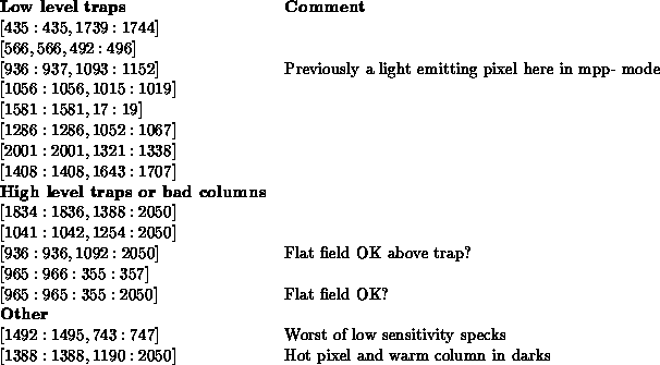
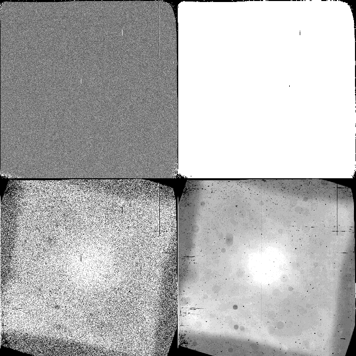
Charge traps and bad columns can be found by comparing a flat field exposure
at very low illumination level to a well exposed one, as illustrated in
figure 1.
In the table below, the coordinates of defects found are listed. Note that
the number of pixels affected by a trap depends on the illumination. The
actual trap location is the smallest Y-coordinate of the area.


Figure 1:
Low illumination level flat field properties, as a mean of identifying
charge traps.
Lower left: Flat field at an illumination level of 74 /pixel.
Grey scale cuts are
  5% of median level.
Lower right: Flat field at an illumination level of 40.000
 /pixel.
The tilted square and central blob structure are caused by stray light in
the setup.
Upper left: Ratio of the two flat fields. The bright vertical lines
show areas affected by low level traps.
Grey scale cuts are
  15% of median level.
Upper right: Different cuts applied to the ratio image, isolating traps


Next: Read-out noise
Up: Properties of
CCD no.
Previous: Operating options
Tim Abbott
Fri Apr 9 15:11:52 ACT 1999
 the non-uniformities
increase to 10%.
At the extreme corners and edges, sensitivity
goes down as the chip is not thinned here. An X-like structure is seen from
corner to corner - this is most probably light reflected off the concave border
to the thinned area at the corners.


 /pixel.
Grey scale cuts are
  5% of median level.
Lower right: Flat field at an illumination level of 40.000
 /pixel.
The tilted square and central blob structure are caused by stray light in
the setup.
Upper left: Ratio of the two flat fields. The bright vertical lines
show areas affected by low level traps.
Grey scale cuts are
  15% of median level.
Upper right: Different cuts applied to the ratio image, isolating traps